

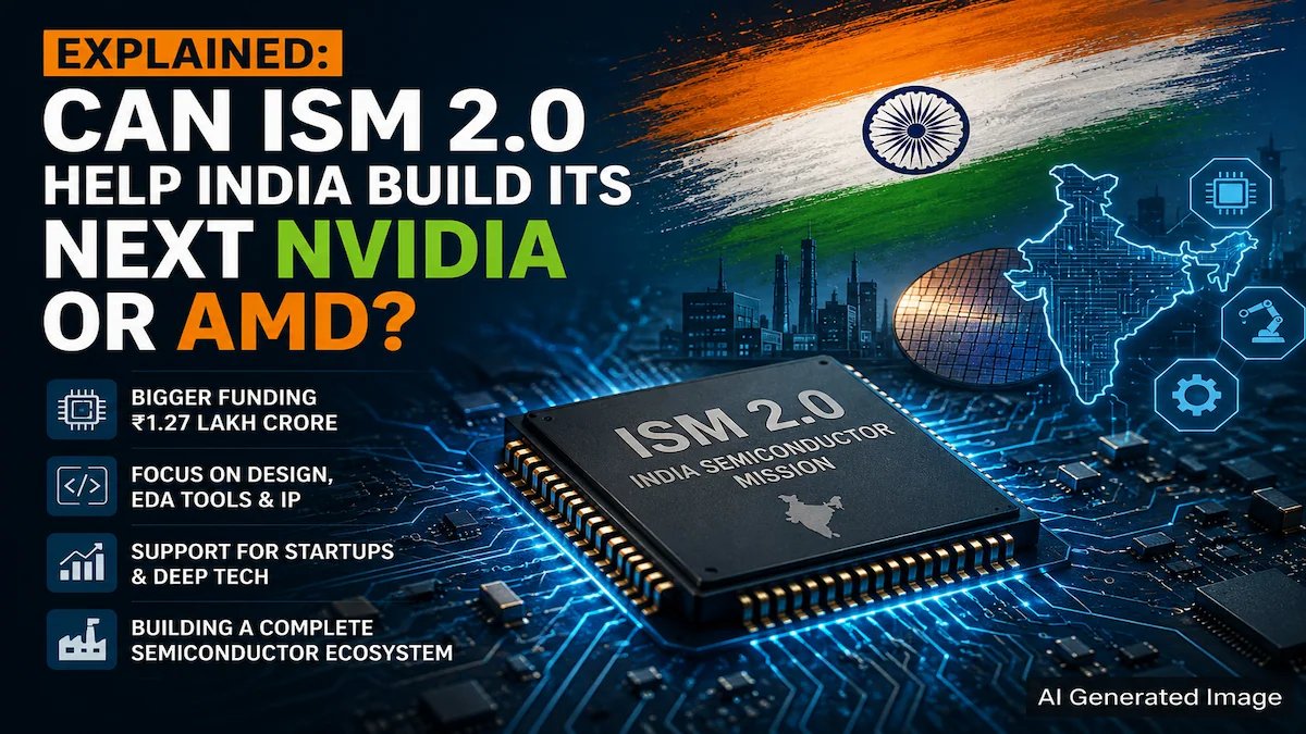
The Union Cabinet on July 15 approved the second phase of the India Semiconductor Mission (ISM 2.0) with a ₹1.27 lakh crore outlay — nearly 1.7 times the ₹76,000 crore allocated under the first phase.
But the significance of ISM 2.0 lies not just in the size of the allocation. The bigger shift is in the scope of the mission.
While the first phase focused largely on building semiconductor manufacturing capacity, the second phase is expected to take a broader approach — covering chip design, electronic design automation (EDA) tools, semiconductor equipment, materials and startups.
The ambition is therefore moving beyond simply making chips in India.
India wants to build a complete semiconductor ecosystem — and, eventually, companies that can develop globally competitive semiconductor technologies.
That raises a larger question: Can ISM 2.0 help India build its next NVIDIA or AMD?
The short answer is that the scheme cannot create a global chip giant by itself. But it could help address some of the biggest structural barriers that have historically made it difficult to build semiconductor companies in India.
Why is ISM 2.0 important?
India’s semiconductor push began with the first phase of ISM, launched in 2021, when the government sought to create domestic semiconductor manufacturing and design capabilities.
The initial focus was understandably on building the physical infrastructure required for the industry. Semiconductor fabrication plants require billions of dollars of investment and highly specialised infrastructure.
But a semiconductor industry cannot be built with fabs alone.
It also needs chip designers, intellectual property providers, equipment manufacturers, materials suppliers, testing and packaging companies, engineering talent and startups that can develop new technologies.
That is where the second phase is expected to be different.
According to Rajan Anandan, MD of Peak XV Partners, India had virtually no semiconductor startup ecosystem six years ago. Today, the country has more than 40 funded fabless semiconductor companies.
“Six years ago, India didn’t have a semiconductor industry. Today, we are well on our way to actually having a semiconductor industry,” Anandan said in an interview with CNBC-TV18.
The ecosystem is now developing across several parts of the value chain, from fabless chip design to fabrication and semiconductor equipment.
The government expects ISM 2.0 to attract nearly ₹4 lakh crore in investments over its 10- to 12-year horizon. It is also expected to generate semiconductor production worth around ₹2 lakh crore and exports of about ₹1 lakh crore over its lifetime.
The objective, therefore, is shifting from building semiconductor factories to building semiconductor capabilities.
How is ISM 2.0 different from the first phase?
The first phase was largely about creating the foundation for semiconductor manufacturing in India.
The second phase is expected to broaden that approach.
The difference can broadly be understood this way:
- ISM 1.0: Build manufacturing capacity and attract large semiconductor projects.
- ISM 2.0: Build a wider ecosystem covering design, equipment, materials, intellectual property and startups.
This distinction matters because the semiconductor industry is not a single business.
A company can design a chip without manufacturing it. Another company can manufacture chips designed elsewhere. Other companies can supply the equipment, materials and software needed by both.
For India to become a serious semiconductor hub, it needs to participate across this entire value chain.
For startups, the structure of support could be as important as the size of the financial allocation.
The government is expected to provide support for semiconductor design, including access to expensive EDA tools. It is also considering co-investment support, where public capital could be invested alongside private investors.
Both could address major barriers faced by early-stage semiconductor companies.
Why are EDA tools so important?
A semiconductor is designed long before it is manufactured.
Engineers need specialised software to create the chip architecture, simulate how it will work, verify the design and identify errors before the design is sent for manufacturing.
These tools are known as electronic design automation, or EDA, tools.
They can be extremely expensive, particularly for startups that may have limited revenue and are still developing their first products.
Shashwath TR, Co-Founder of Mindgrove Technologies, said access to EDA tools had played an important role in enabling the company to develop its semiconductor technology.
“Mindgrove would not exist today without that EDA tool support,” he said.
For an early-stage company, government support for EDA tools can reduce the amount of capital that has to be spent on basic infrastructure.
That allows a startup to deploy more of its funding towards engineering, product development, testing and commercialisation.
Support for intellectual property and specialised expertise could also be important.
A chip company does not necessarily have to develop every component of a design from scratch. It can license certain technology blocks, or IP, and focus its resources on the parts that provide its competitive advantage.
Reducing the cost of accessing these tools and capabilities could help more Indian semiconductor startups move from an idea to a working product.
Why could government co-investment matter?
Semiconductor startups are capital-intensive businesses.
The cost of designing, testing and manufacturing a chip can be substantial even before a company begins generating meaningful revenue. As a result, startups often require multiple rounds of funding over several years.
This creates a funding challenge.
Venture capital investors may be willing to fund early-stage design companies, but the amount of capital required to develop semiconductor technologies can be significantly higher than for many software startups.
This is where government-backed co-investment could potentially play a role.
However, the structure of such support will be critical.
Dheemanth Nagaraj, Co-Founder and CEO of Agrani Labs, said government participation could be useful as long as it does not affect the control and independence of the founding team.
“For us to be competitive on the world stage, we have to be on a leading process node,” Nagaraj said.
He also suggested that a mechanism allowing a company to buy back the government’s stake at reasonable terms could make such an arrangement more attractive to founders.
The concern is important. A government stake could have implications for future fundraising, ownership, governance and decision-making.
Anandan argued that government co-investment should be viewed as an option rather than a mandatory requirement.
A startup that does not want to access government-backed capital should not be forced to do so.
He also pointed to the Research Development and Innovation (RDI) scheme as a possible model. Under such a structure, companies could potentially repay part of the capital at a later stage, while the government retains a smaller stake.
The broader principle is straightforward: public capital can help reduce the early risks of building semiconductor companies, but it should not replace private capital or entrepreneurial decision-making.
The fine print will determine whether the model actually works.
Why is the fabless model important?
One of the most important ways India could build globally competitive semiconductor companies is through the fabless model.
A fabless company designs chips but outsources their manufacturing to semiconductor foundries.
This allows the company to focus on chip architecture, intellectual property and product development without having to build and operate its own fabrication plant.
NVIDIA and AMD are examples of companies that primarily operate through this model.
This is important because India does not need to build a fabrication plant for every successful semiconductor company.
A startup can potentially design a chip in India, manufacture it through a global foundry and sell the finished product to customers around the world.
But a successful fabless semiconductor company requires more than engineers.
It needs access to EDA tools, intellectual property, capital, advanced manufacturing capacity, testing and packaging facilities, and customers willing to adopt its products.
This is why a broad ecosystem is important.
The more of these capabilities that are available to Indian companies, the lower the barriers to building globally competitive semiconductor products.
Why do leading-edge process nodes matter?
Capital and talent alone will not be enough to create a global semiconductor champion.
The technology used to manufacture a chip also matters.
Agrani Labs is developing a GPU aimed at competing in the global artificial intelligence market. Nagaraj said access to advanced manufacturing technology would be essential for the company’s ambitions.
“For us to be competitive on the world stage, we have to be on a leading process node,” he said.
Leading-edge process nodes allow manufacturers to produce smaller, more powerful and more energy-efficient chips.
However, developing these capabilities is extremely difficult and expensive.
The most advanced semiconductor manufacturing capabilities are concentrated among a small number of companies and countries, including Taiwan, South Korea and the United States.
India is building its domestic semiconductor manufacturing ecosystem, but reaching the cutting edge of process technology will be a long-term challenge.
Nagaraj said India’s leading-edge chips may initially need to be manufactured through global foundry partners such as TSMC or Intel.
Over time, however, the expansion of India’s fabrication and semiconductor materials ecosystem could help the country develop increasingly advanced domestic capabilities.
This is unlikely to be an immediate outcome of ISM 2.0.
Building leading-edge semiconductor manufacturing requires years of investment, technology development and operational expertise.
Does India have the talent to build global chip companies?
Capital and infrastructure will not be enough.
The semiconductor industry requires highly specialised engineers, including chip designers, verification engineers and experts in areas such as artificial intelligence hardware.
According to Anandan, around 20% of the world’s semiconductor designers are based in India.
The challenge is that many of these engineers currently work for global companies such as NVIDIA, Intel and AMD.
The opportunity for India is to encourage more of this talent to build companies in the country.
Anandan said experienced engineers are increasingly leaving global technology companies to launch startups in India.
The same movement is also taking place in academic institutions.
Mindgrove was founded by entrepreneurs connected to IIT Madras, while the IIT Madras Research Park has become an important hub for deep tech startups.
This movement of talent from multinational companies and academic institutions into startups could be one of the most important outcomes of India’s semiconductor push.
A country does not build a global semiconductor company simply by having engineers.
But it is unlikely to build one without them.
Can ISM 2.0 create India’s next NVIDIA or AMD?
This is where the comparison needs to be treated carefully.
NVIDIA and AMD were built over decades. Their competitive advantages extend far beyond chip design.
They include semiconductor architecture, intellectual property, software ecosystems, developer platforms, access to advanced manufacturing, large research and development budgets and deep relationships with customers.
Government support cannot replicate all of these capabilities overnight.
ISM 2.0 also cannot guarantee that a particular Indian startup will become a global technology leader.
What it can potentially do is reduce some of the structural barriers that make semiconductor entrepreneurship difficult.
These include:
- The high cost of EDA tools and chip design
- Limited access to semiconductor IP
- The shortage of early-stage deep tech capital
- The cost and complexity of testing and manufacturing
- Limited access to advanced process nodes
- The need to develop a wider equipment and materials ecosystem
- The challenge of retaining and attracting specialised engineering talent
Anandan said ISM 2.0 could accelerate the development of multiple parts of the semiconductor value chain, including equipment.
“The train has left the station. Indian deep tech is at the early stages, but we can’t be more excited about both the talent as well as the ecosystem,” he said.
That may be the most important way to view the second phase of India’s semiconductor mission.
ISM 2.0 cannot create India’s next NVIDIA or AMD by itself. But it could help create the conditions in which such companies can be founded, funded, developed and scaled in India.
The immediate goal, therefore, is not to replicate a company that took decades to build.
It is to ensure that the next generation of Indian semiconductor startups has access to the tools, capital, talent, infrastructure and manufacturing partnerships needed to compete globally.
If that ecosystem develops successfully, India’s future semiconductor champions may not simply manufacture products for global companies.
They could be designed, headquartered and built in India.
Why the wider electronics ecosystem also matters
The semiconductor push is also being paired with a broader effort to expand electronics manufacturing.
The Union Cabinet has approved a ₹62,500 crore mobile manufacturing scheme for five years. The scheme is expected to generate mobile phone production worth nearly ₹39 lakh crore, boost exports and create around 60,000 direct jobs.
This matters because semiconductors do not exist in isolation.
A broader electronics ecosystem creates potential customers, suppliers and manufacturing partners for semiconductor companies.
The combination of semiconductor support and mobile manufacturing incentives is therefore aimed at building a wider chain — from chip design and components to manufacturing and exports.
For India, the larger ambition is to move beyond being a major consumer and assembler of technology products.
The challenge is to become a country where advanced technologies are also designed, developed and commercialised.
ISM 2.0 is an attempt to build the infrastructure and financial support for that transition.
Whether it produces India’s next NVIDIA or AMD will depend on what companies, technologies and entrepreneurs emerge over the next decade.
But the policy shift is clear: India is no longer only trying to attract semiconductor factories. It is trying to build the ecosystem from which globally competitive semiconductor companies can emerge.
Watch accompanying video for full conversation.